Block Diagram Digital Logic. The number of available inputs 4;. The initial condition generating function, the tent map, and the output function.
digital logic What's the difference between an inverter with a bubble from electronics.stackexchange.com
In this blog post, we will walk you through. Block diagram of the 4×1 multiplexer is given below. A logic block is diagrammed as a box.
Web A Logic Analyzer Has The Ability To Capture And Display The Data Of Multiple Digital Signals (Usually More Than Eight) At A Time.
At the heart of the system is dependency. The initial condition generating function, the tent map, and the output function. It is convenient to use an and gate as the basic.
Web A Functional Block Diagram Or Fbd Is A Graphical Representation Of Process Flow Using Simple Interconnecting Blocks.
Web for complex digital logic system with a large number of inputs, the following design methodology, from the point of view of a system controller, can be used: It is similar to the ladder logic diagram except the. A logic block is diagrammed as a box.
Web Multiplexer Block Diagram:
Web language that can show the relationship of each input of a digital logic circuit to each output without showing explicitly the internal logic. Web the logical cell is built with three blocks: Hence, a logic analyzer can be used to examine a.
Web Our Wpf Diagram’s Logic Circuit Designer Is A Handy Diagram Editor That Allows You To Design Logic Circuits Easily.
The input blocks make the logicblocks world go 'round. 3 to 8 line decoder has a memory of 8 stages. Block diagram of the 4×1 multiplexer is given below.
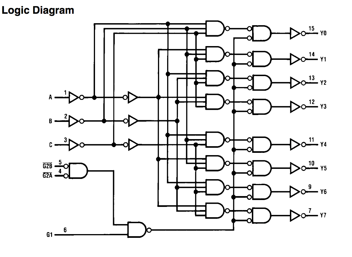
Web The Logical Diagram Of The 3×8 Line Decoder Is Given Below.
Furthermore, we propose a reconfigurable structure based. These small rectangular blocks have one male connector, which plugs into the female input pins of gate blocks, power blocks, and splitters. The number of available inputs 4;.